French Deeptech cluster


French Deeptech cluster
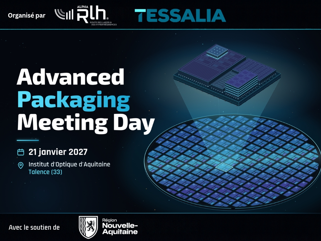
Advanced Packaging is expanding beyond its original field—microelectronics—to shape a new value chain in the manufacturing of highly integrated electronic systems.
The approach of integrating an entire system onto a single chip (SoC—System on Chip) is now reaching its limits in terms of cost and efficiency, gradually giving way to approaches based on smaller, optimized chips known as “chiplets.” This shift presents a real opportunity for European players in the semiconductor and integrated systems sectors to strengthen their autonomy.
One of the goals of advanced packaging is to integrate multiple chips onto a given surface area to create a complete system in a single package (SIP—System in Package) that is smaller, lighter, and offers unprecedented cooling capabilities. Finally, because some of the complexity of the underlying PCB is transferred to the substrate, the SIP simplifies the PCB’s design.
The targeted applications include HPC computing, AI servers, real-time computers, defense, healthcare, energy, and more . In practice, this applies to all sectors that require high processing power in a small space.
Take advantage of this spotlight on this true bridge between chips and systems, and come meet the leaders in these technologies at the “Advanced Packaging Meeting Day” event .
On the agenda: a detailed presentation of TESSALIA (Thales/Radiall/Foxconn), the future sponsor of this event, and its planned factory in the town of Le Barp (33). The day will also feature presentations by the SERMA Group, CEA-Leti, and other industry players, as well as time set aside for discussions and networking among participants.
Contact ALPHA-RLH: l.dugoujon@alpha-rlh.com


